Premium and Platinum tiers
From $3 billion to $91 billion market: A deep dive into the photonics value chain
The AI connectivity market is set to grow rapidly over the next three years. This deep dive covers everything you need to know about the industry and the best positioned businesses to benefit as demand grows exponentially

Note: the semiconductor industry is a highly technical one. Throughout this deep dive, there are a lot of technical concepts that I'll try to explain the best I can. The glossary below covers the most important technical concepts mentioned in this piece.
Semiconductor glossary
- Optics / optical (interconnect, module, engine, filter): Data transmission using light instead of electricity, enabling much higher speeds and longer distances than copper without signal degradation
- Copper cable: Traditional electrical cable used inside data centers; fast over short distances but loses signal integrity as speeds and reach increase
- Photonics: The science and engineering of generating, controlling, and detecting photons to transmit and process information at high speed
- Co-packaged optics (CPO): Advanced packaging that integrates optical engines directly onto the same substrate as the switch chip, cutting power use and signal loss versus pluggable modules.
- Laser: A device producing a focused, coherent beam of light that serves as the carrier signal onto which data is encoded
- Indium phosphide (InP): Compound semiconductor material used as the substrate for the highest-performance lasers and photodetectors in optical communication
- Substrate / wafer: A thin, polished disc of semiconductor material that acts as the physical foundation on which transistors, lasers, or photonic circuits are built
- Optical engine: The core optical sub:assembly inside a CPO module that handles light generation, modulation, and detection in a compact integrated package
- Transceiver: A combined transmitter and receiver module that handles both sending and receiving of optical data signals
- Continuous-wave (CW) laser: A laser emitting a steady, uninterrupted beam of light, used as the external light source in CPO architectures
- Electro-absorption modulated laser (EML): A laser with a built-in modulator on the same chip, widely used in high-speed transceivers and now being partially displaced by silicon photonics
- Silicon photonics (SiPh): A technology that manufactures photonic components using standard silicon semiconductor processes, enabling lower-cost, high-volume production
- Scale-up networking: High-bandwidth connections linking GPUs within a single rack so they operate as one unified computing system
- Scale-out networking: Connections that link multiple racks or clusters into a larger distributed compute fabric, typically handled by 800G+ optical modules
- Modulator: A component that rapidly switches a laser beam to encode digital ones and zeros onto the light signal
- Photodetector: A component that receives incoming light signals and converts them back into electrical signals a processor can read
- Total addressable market (TAM): The total revenue opportunity for a product or technology if every potential customer adopted it
- Wafer probe / wafer-level test: Electrical and optical testing performed directly on a wafer before dicing, catching defects before expensive downstream steps
- Lithography (EUV): A manufacturing step that uses light to project circuit patterns onto a wafer, with EUV using very short wavelengths to print the smallest features
- Yield management: The practice of identifying and eliminating defects as early as possible in production to maximize the share of working chips per wafer
Introduction
A few weeks ago, Goldman Sachs published an equity research report about optical networking: "the next megatrend in AI". One line inspired me to write this deep dive:
A 13x larger addressable market for optical modules / optical engines (...) and a 10x larger value market for pluggable optical modules (...) in 2028 ~ Goldman Sachs
That got me thinking about the road ahead. The GPU's are the compute brain but you also need a nervous system connecting it all together. What exactly does that look like and who owns the parts of that nervous system that cannot be copied in a year or two?
This deep dive is my answer to that question. I'll walk through the physics, the five layers of the photonics stack, the chokepoints, the names I personally own and those on my watchlist. With that being said, let's start with the problem itself.
1 - The problem
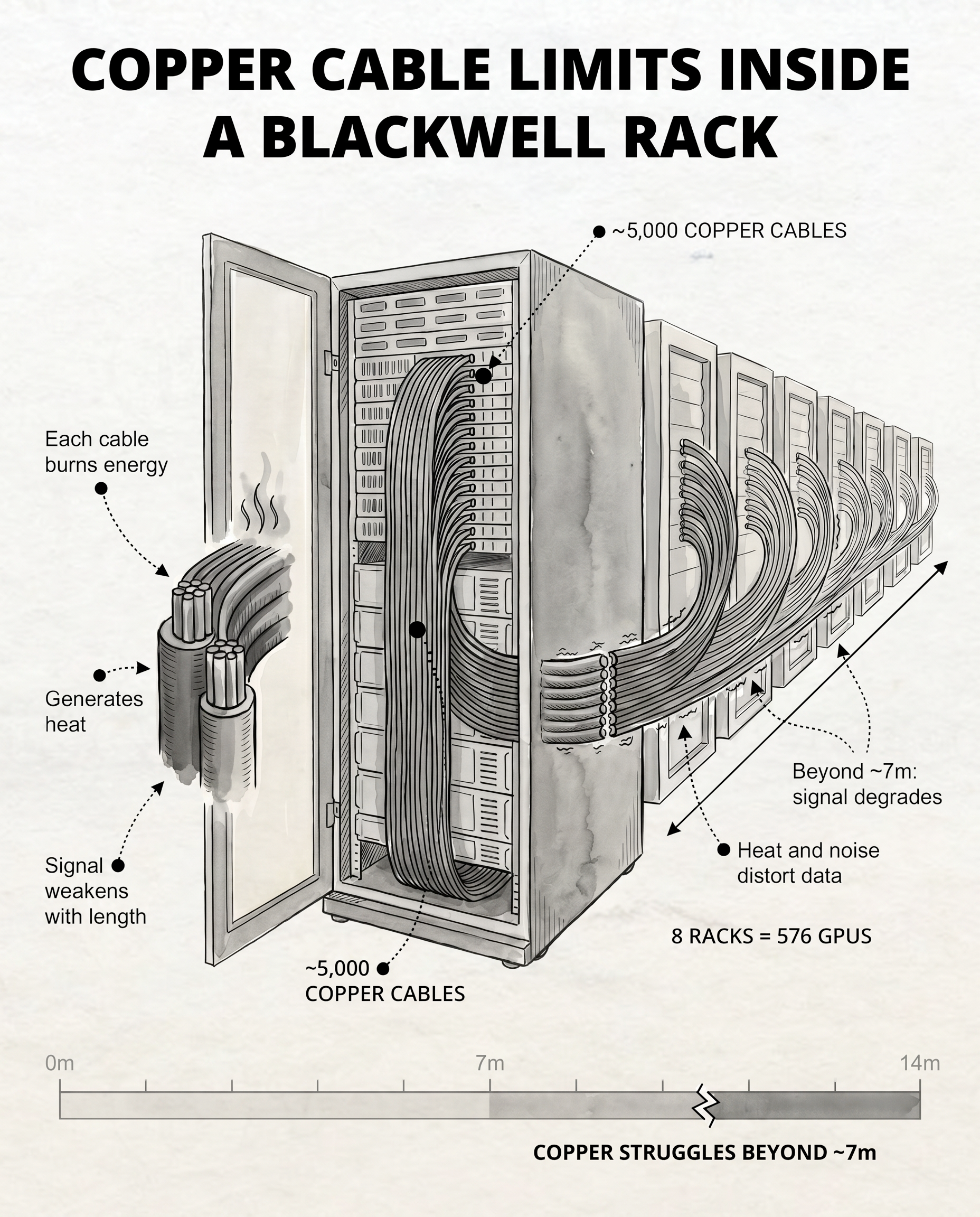
AI data centers are no longer compute bound. They're connectivity bound. Copper cables (the traditional electrical wires inside server racks) used to be enough. They could push 800 gigabits per second over short distances, which sounds like a lot until you see what an AI cluster actually demands.
The faster you push, the shorter the cable can be before the signal falls apart. That's not simply an engineering problem someone can solve with better insulation.
💡
Speeds are often referred to in "G's", meaning gigabits. If you divide that by 8, you get the speed in gigabytes. So 400G = 50GB, 800G = 100GB etc.
The visual below is an illustration what a Nvidia Blackwell rack looks like. Inside, there are roughly 5,000 copper cables, the nervous system connecting all the GPUs together. Every one of them is burning energy, throwing off heat, losing integrity past about seven meters.
That's where optics take over. Light doesn't degrade the same way over distance. It runs cooler and it carries more data.
The way I see it, we're in a moment of time where the bottleneck and the solution are both physical, visible, and still in the the early innings of a multi year ramp.
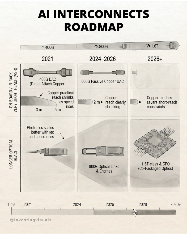
2 - The connectivity timeline
The connectivity timeline consist of three phases, each one extending the previous:
- 2021: max speeds around 400G, copper handling 3 to 5 meter links. That's the equivalent of streaming 100 HD movies every second
- 2024 to 2026: copper pushed to 800G but reach shrinks to about 2 meters
- 2026 and beyond: copper hits its physical limit, optics take over up to 1.6T over both shorter and longer distances
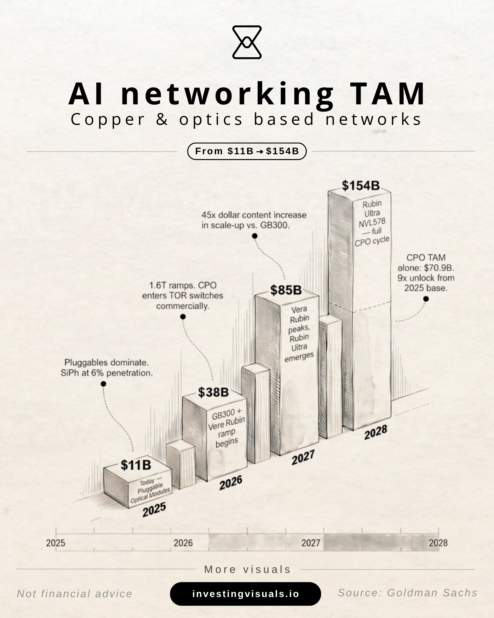
The combined connectivity TAM (copper + optics) is forecast to grow from roughly $11B today to $154B at full buildout.
- Copper based: $8B → $34B (4x)
- Optics based: $3B → $120B (40x)
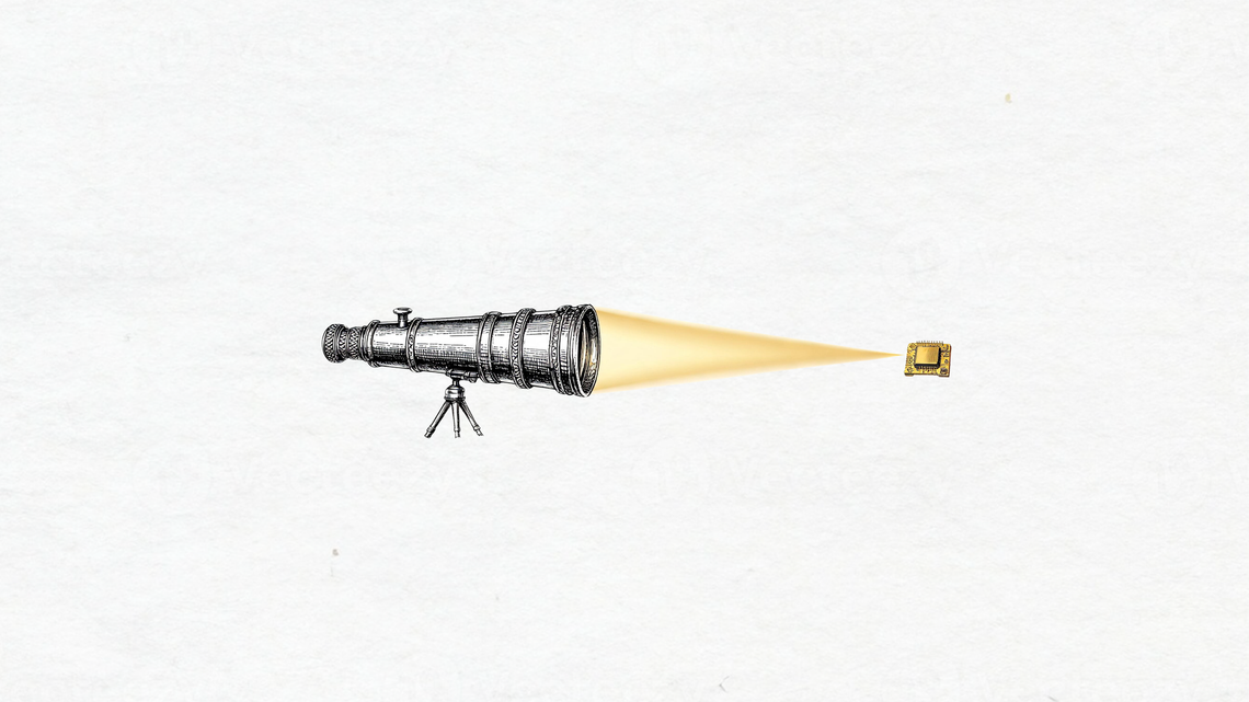
Given the 40x of optics, this deep dive focuses on just that, specifically photonics: the science of using light (photons) to move data. But before naming any businesses, it's important to understand the industry stack. So let's look at how it actually works.
Let there be light
3 - How photonics work
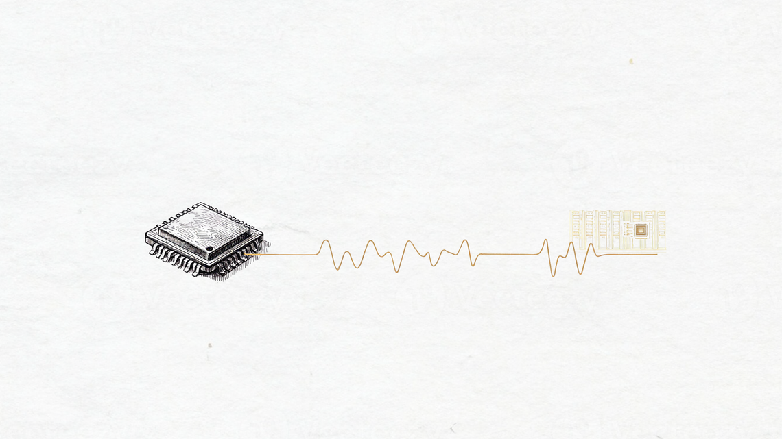
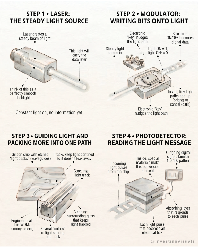
Photonics is using light to carry information. Sounds simple right? The engineering behind it is anything but.
You take a laser beam. You encode ones and zeros onto it. You transmit that light at speeds copper cannot match and four components have to work in tight coordination to do so.
- Laser: creates a steady beam, the carrier signal
- Modulator: takes that steady beam and switches it on and off fast enough to encode data
- Waveguides and wavelengths: tiny pathways guiding light across a chip, multiple colors traveling the same route at once
- Photodetector: receives the light and converts it back into an electrical signal the computer can read
Pull any one of these out and none of it works anymore. That mutual dependency is exactly what makes the supply chain so interesting.
4 - The five layers of the photonics value chain
To make photonics work at scale, you need a lot of highly specialized businesses operating across a deeply layered supply chain. I find it useful to think of it as five distinct layers, because where a business sits in that stack tells most of what you need to know about its margin profile, its moat, and how defensible its position really is.
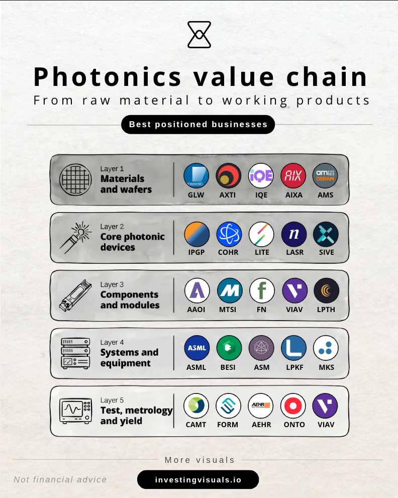
Layer 1 - Materials and wafers
Everything starts here. Raw material gets converted into ultra clean surfaces for light based devices. It's the canvas before anyone paints. A single defect at this level compounds through every step downstream.
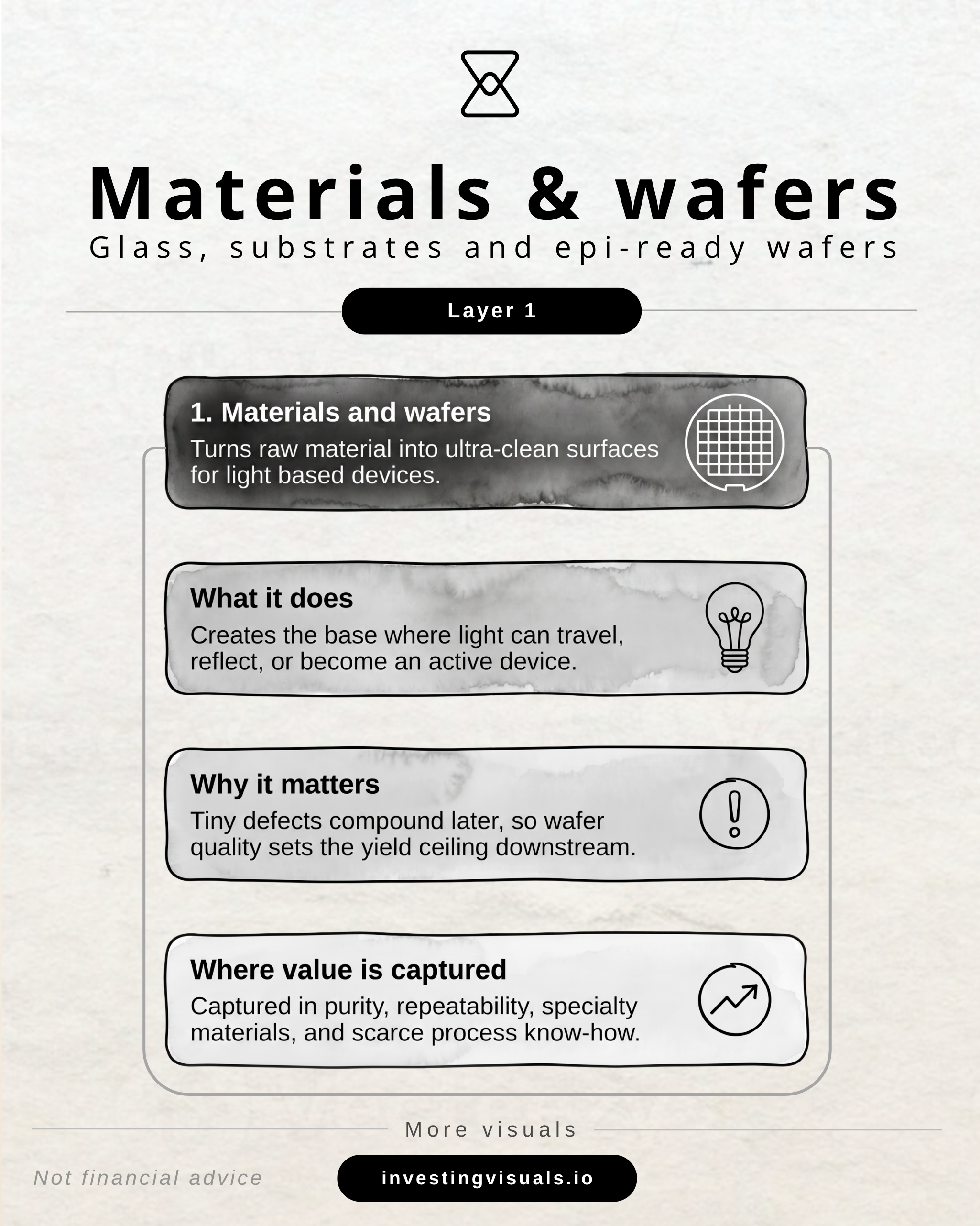
The critical material in AI photonics isn't silicon. It's indium phosphide, InP. InP wafers are the substrate (a thin slice of semiconductor that acts as the foundation) for the lasers and photodetectors that make high speed optical communication possible.
InP wafer capacity needs specialized equipment, process expertise that takes years to build, and customer qualification cycles that run 12 to 18 months. You can't turn this market on with a capital injection and a factory lease and call it a day.
Key businesses:
- Corning (GLW): dominant optical fiber and specialty glass, Goldman models 1,152 fiber units per CPO switch at $11 average selling price
- AXT (AXTI): with Sumitomo Electric controls roughly 78% of global InP substrate output, a functional duopoly
- IQE: leading compound semiconductor wafer supplier
- Aixtron (AIXA): makes MOCVD systems used to deposit thin material layers
- ams OSRAM (AMS): global leader in optical solutions and sensing
Value in this part of the chain comes from purity, repeatability, and scarce process know how. There are high switching costs, long qualification cycles and businesses are highly specialized.
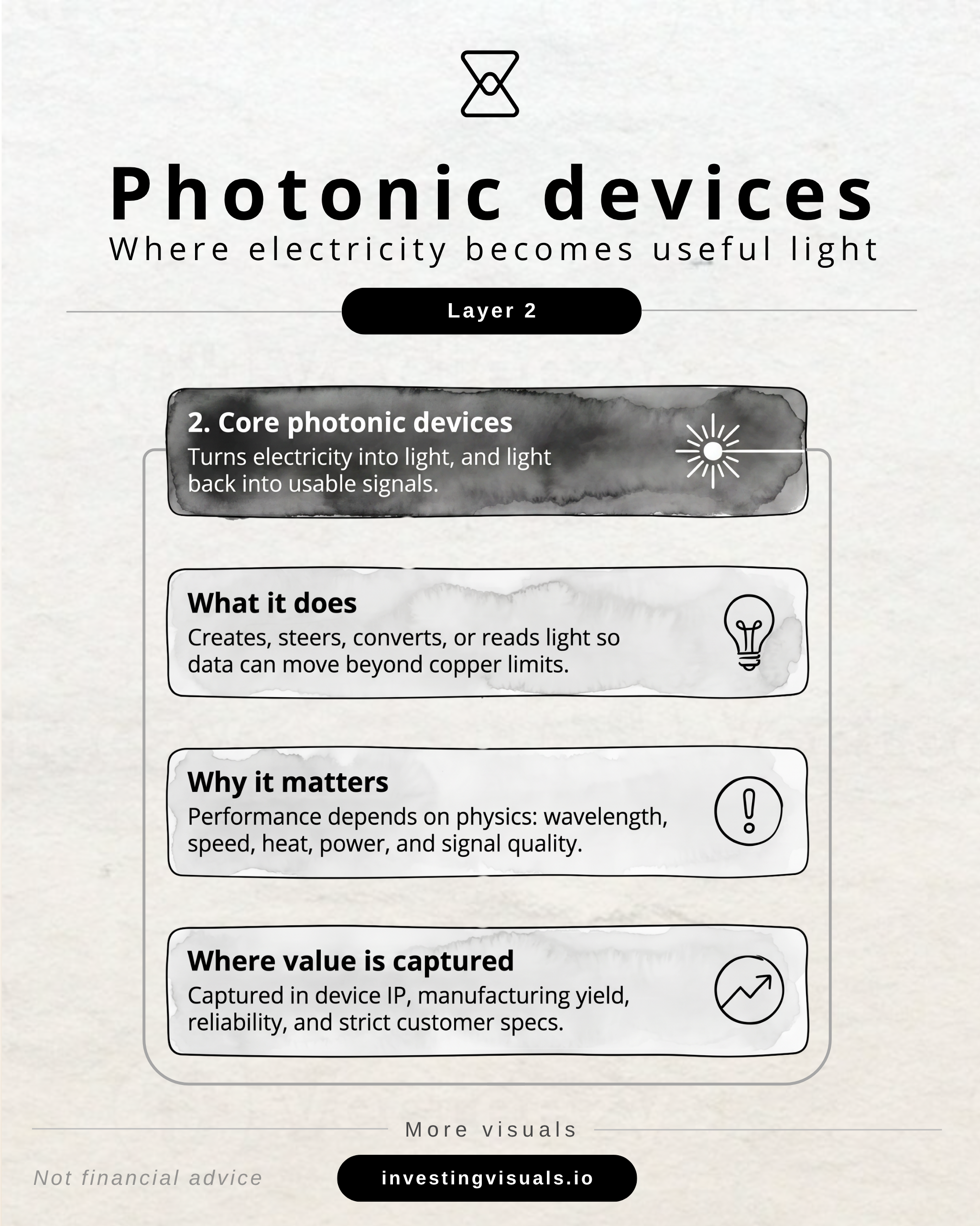
Layer 2 - Core photonic devices
This is where the physics happens. Layer 2 converts electricity into light and light back into electrical signals. Performance depends on wavelength, speed, heat, power consumption, and signal quality.
Two transitions are reshaping this layer right now.
First: the shift from electro absorption modulated lasers (EML) toward silicon photonics (SiPh). Goldman models SiPh penetration growing from 6% in Q1 2024 to 46% by Q4 2028. The economics behind this; SiPh costs 26% less than EML at 800G and 32% less at 1.6T.
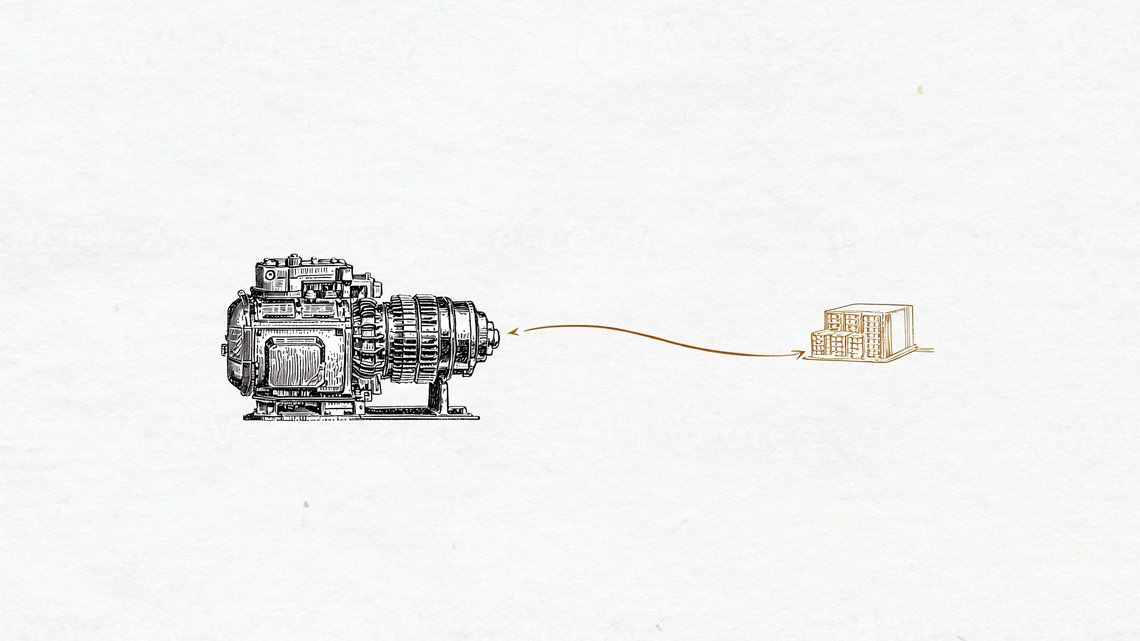
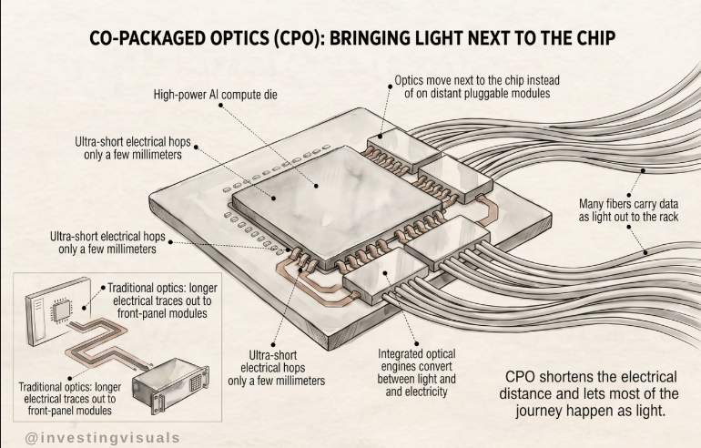
Second: the move toward continuous wave (CW) integrated laser sources for co-packaged optics (CPO) architectures. CPO integrates the optical engine directly onto the same substrate as the switch chip. That makes integrating the laser inside impractical, so external laser sources become mandatory.
Here's a number that is particularly interesting for businesses operating in this layer: The Nvidia Quantum X Photonics CPO switch uses 18 external laser sources. Broadcom's Spectrum X Photonics uses 64. Multiply that across millions of ports and laser supply in particular becomes the defining constraint on how fast this whole ecosystem can scale.
What co-packaged optics looks like in real life:
Key businesses:
- Coherent (COHR): the vertically integrated player, lasers, optical components, transceivers, SiPh devices, all under one roof
- Lumentum (LITE): major CW and EML laser supplier with a 40% capacity expansion underway
- IPG Photonics (IPGP): high power fiber lasers, mostly industrial and medical
- nLIGHT (LASR): fiber laser maker with defense and industrial applications
- Sivers (SIVE): makes InP laser chips and photonic integrated circuits used as light sources inside transceivers and CPO modules
In Layer 2, value sits in device IP, manufacturing yield, reliability, and customer qualification lock in. Getting designed in takes about a year. Getting swapped out takes a lot longer.
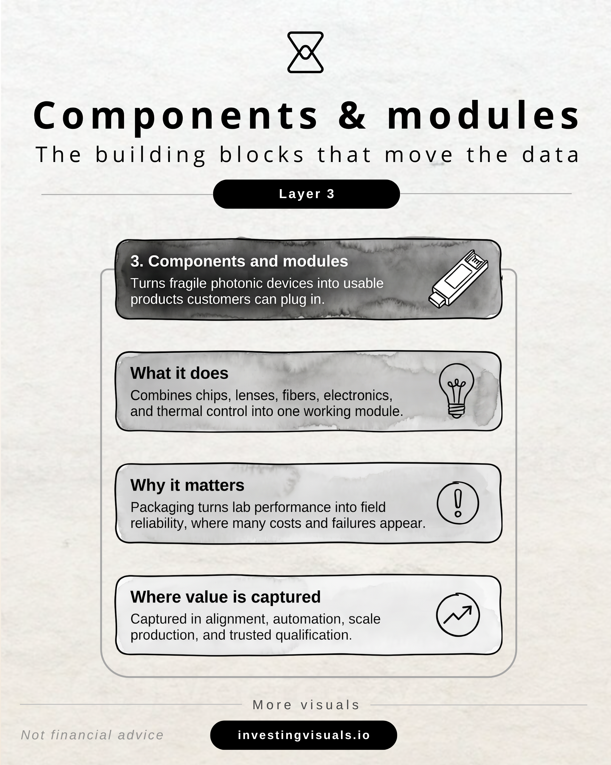
Layer 3 - Components and modules
Layer 3 takes the photonic devices from Layer 2 and packages them into something a customer can actually plug in. Chips, lenses, fibers, electronics, thermal control, all integrated into a single working module.
The speed migration here is sequential and quite predictable. 800G is mainstream in 2025. 1.6T takes over through 2026. 3.2T enters volume ramp from 2027 onward.
Each generation is a potential gross margin expansion event for suppliers who've made the photonics transition. Goldman models optical module supplier margins ramping toward 48% to 55% as the mix shifts toward higher speed photonics.
A dynamic that I find particularly interesting is "GPU attach rate": the number of high-speed optical transceivers or photonic connections required to support a single Graphics Processing Unit. In the NVIDIA GB300 rack, each GPU has 3 optical modules. In Vera Rubin (2026), that doubles to 6. That's a 2x revenue multiplier on the existing market from a single GPU generation transition, with no market share gains required.
Key businesses:
- Applied Optoelectronics (AAOI): transceiver maker with direct hyperscaler exposure
- MACOM (MTSI): amplifiers and drivers inside transceivers
- Fabrinet (FN): the contract manufacturer for optical components, the TSMC of photonics packaging
- Viavi (VIAV): provides network test, monitoring, and assurance solutions along with optical security and performance products
- Lightpath (LPTH): proprietary optical and infrared components
Value here is captured in precision alignment, automation, scale, and hyperscaler qualification status. Being the sole qualified supplier on a specific module configuration at a Tier 1 customer is about as close to a monopoly as commercial electronics gets.
Layer 4 - Systems and equipment
Layer 4 builds the platforms for production, sensing, imaging, inspection, and data movement. Customers here aren't really buying machines, they're buying uptime, precision, throughput, and a qualified process.
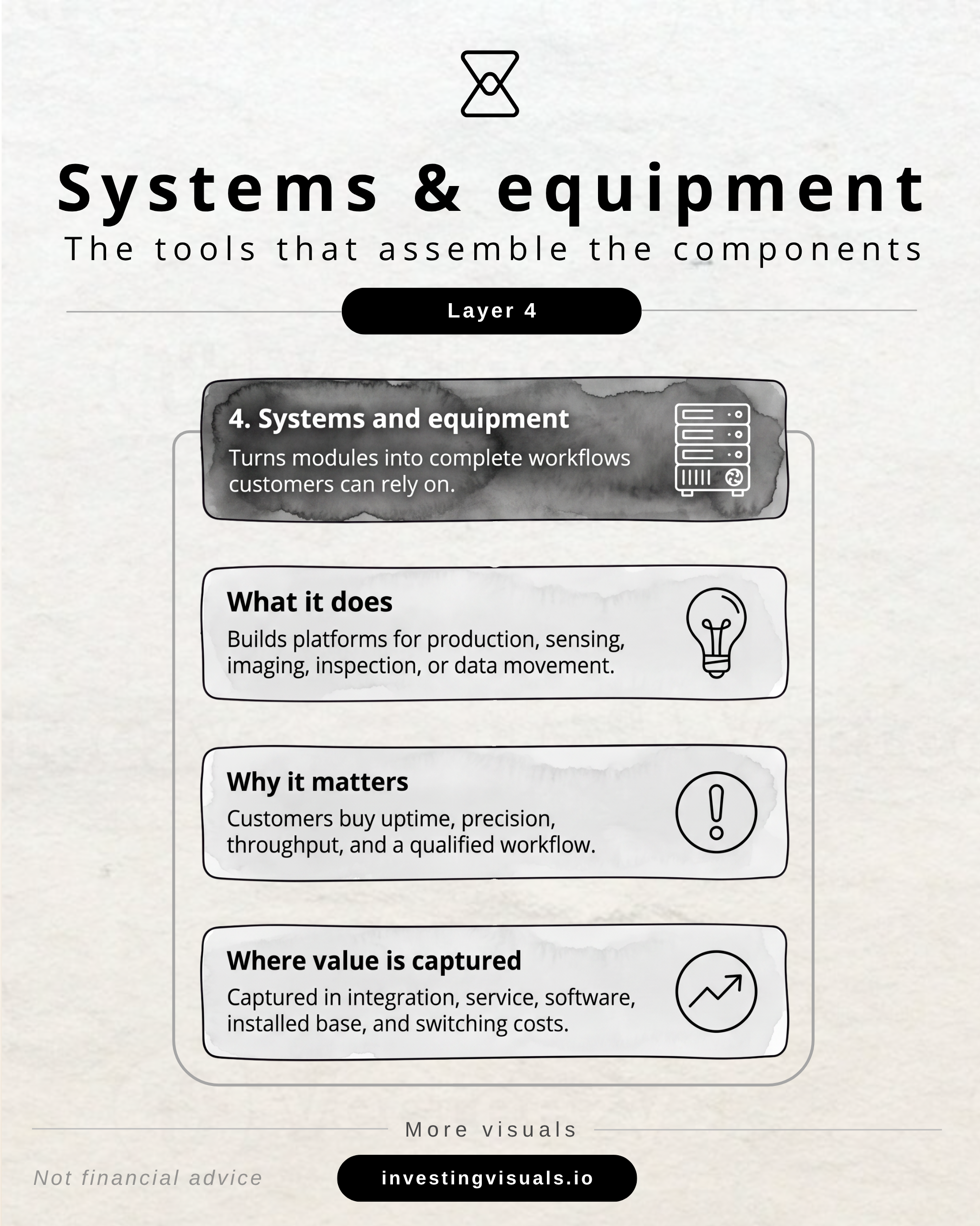
The most consequential transition here is photonic packaging converging with semiconductor grade precision. CPO requires aligning optical engines at micron level tolerances, roughly 1/70th the width of a human hair. That pushes photonic assembly equipment into territory previously occupied only by advanced semiconductor packaging tools.
Key businesses:
- ASML: lithography and inspection, increasingly relevant as photonic ICs adopt semiconductor grade processes
- Besi (BESI): advanced die bonding for chip and photonic packaging
- ASM International (ASMI): thin film deposition equipment
- LPKF Laser & Electronics (LPKF): high precision laser systems for printed circuit boards
- MKS Instruments (MKSI): power and process control systems
Once a production line qualifies a piece of equipment, it doesn't swap mid process. The recurring service and upgrade revenue that follows is highly predictable and largely immune to capex cycle volatility.
Layer 5 - Test, metrology, and yield
Every device and module that moves through the four layers above eventually arrives here. Layer 5 decides whether it meets specification. The economic logic is deeper than just quality control.
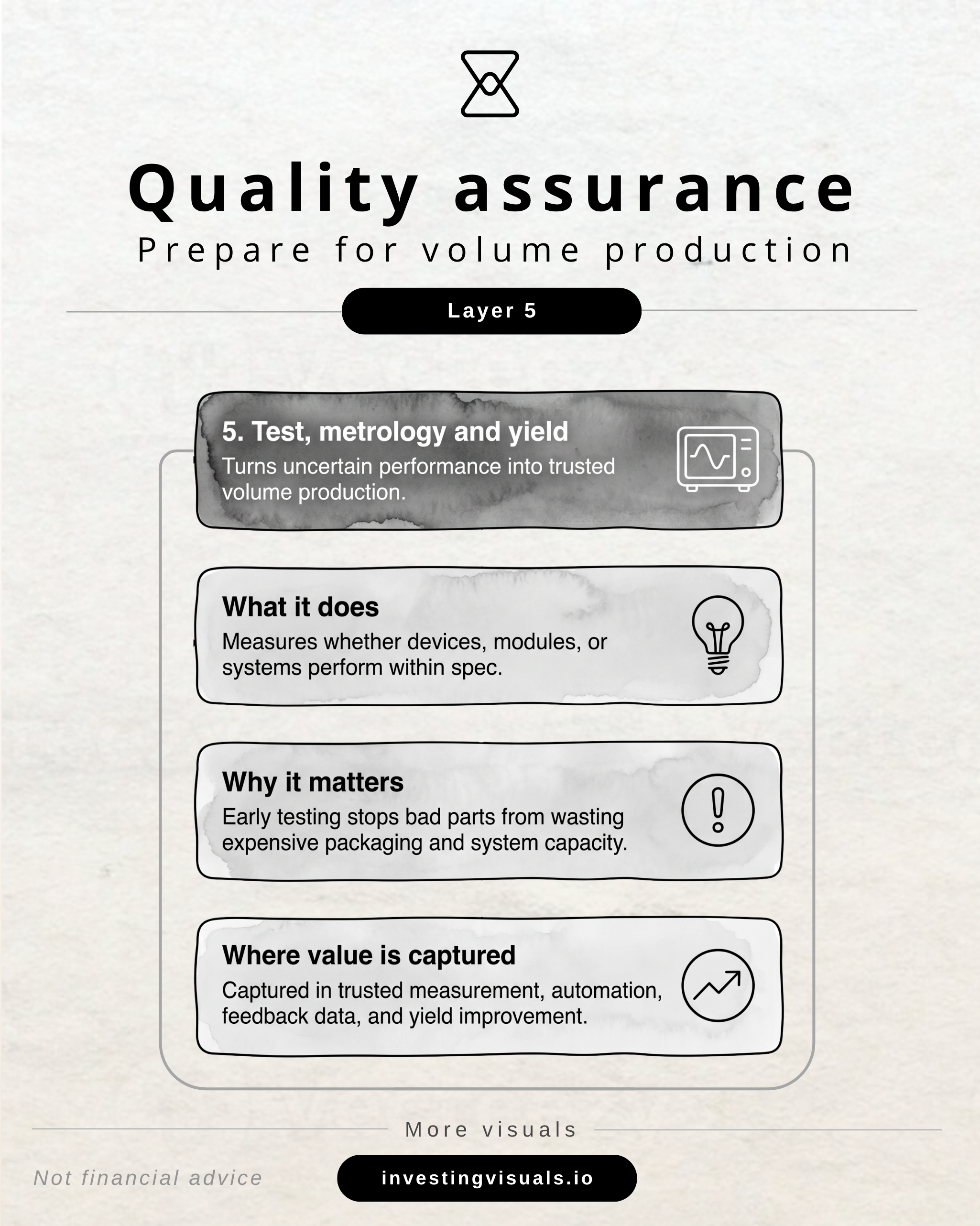
A CPO switch carries a selling price of $130,000 to $500,000. Of that, $32,400 is optical engines alone. If a defective optical engine passes through wafer fabrication, assembly, and packaging before failing at system level test, the entire assembly may need rework or scrap. If you catch that same bad engine at wafer level, none of those expensive downstream steps are triggered.
Yield management, the process of maximizing the share of working chips per wafer, is the difference between a profitable line and a losing one.
Key businesses:
- CamTek (CAMT): sells inspection and metrology equipment
- Viavi (VIAV): optical filters and test equipment
- FormFactor (FORM): wafer probe systems, with a unique commercial answer to electrical and optical testing at the same time
- Aehr Test (AEHR): burn in and reliability testing for SiC and SiPh wafers
- Onto Innovation (ONTO): optical metrology and inspection, sub micron alignment verification for CPO
Changing a test system mid production disrupts yield baselines and triggers full requalification. These businesses have some of the most defensible installed bases in the entire semiconductor supply chain.
What do the years ahead look like?
5 - The roadmap and the risks
I'd normally separate roadmap and risks into two sections. Here, the risks live inside the timeline, so let me walk it forward.
2025–2026: The speed of migration and laser squeeze
Today's most used GPU rack is the GB300, copper is everywhere inside the rack for scale up, 800G and 1.6T optical modules are handling the scale out (multiple racks in parallel). Goldman shows 1.6T moving from roughly 20% market share in Q4 2025 toward mainstream by mid 2026, with 3.2T entering small sample production at the same time.
The constraint isn't demand but the light source supply. As per Goldman Sachs: supply tightness across both EML and CW lasers through 2026, driven by strong AI server demand, InP substrate constraints, and geopolitical export controls on Chinese substrate supply.
Lumentum committed to 40% capacity expansion and Coherent committed to doubling but the semiconductor supply chain expansions take 12 to 18 months from plan to volume.
The risk
If laser supply stays bottlenecked through 2027, it's good for margins but bad for volume. More GPUs means more modules. But no lasers, no modules. I could be wrong on the timing here, but this could very well cap the ramp for a considerable amount of time, pushing the roadmap further into this decade.
2026–2027: Vera Rubin and the CPO commercial inflection
Vera Rubin introduces the first commercial CPO deployment in scale out switches. Goldman assumes 25% CPO penetration at this layer. Nvidia's Quantum X Photonics CPO switch was announced in March 2025 and reaches commercial availability in early 2026. Broadcom's Davisson 102.4T CPO switch was delivered to customers in October 2025.
The risk
CPO requires a full supply chain migration. When a pluggable module fails, you pull it out and simply replace it in seconds. When a CPO optical engine fails inside a co packaged switch, the failure can take down the whole switch. Adoption pace depends partly on component availability and partly on whether network operations teams accept a fundamentally different failure model.
It remains to be seen how fast hyperscalers embrace/mitigate that operational risk.
2027–2028: Rubin Ultra and scale-up
This is where the photonics TAM gets another big bump.
Scale up networking per rack is expected to jump from $140K in GB300 to $803K in Rubin Ultra NVL576, a 5.7x increase. Goldman's CPO TAM estimate for the full Rubin Ultra cycle reaches $70.9B in 2028 in the high end scenario, with optical engines alone contributing $43.9B.
Today's entire optical transceiver market is roughly $8B to $10B annually. The 2028 CPO TAM in the high end scenario is more than 4x the current total market, in a single product category that barely existed commercially in 2025.
The risk
Rubin Ultra is planned for 2027 to 2028. That's quite a long time in AI infrastructure. Training workloads could shift faster toward inference, lowering the demand for massive scale up. Hyperscalers could face capex pressure if AI monetization stretches. Any of those scenarios delays the ramp. Time will tell.
6 - High potential investments
With businesses spread across five layers, it's easy to get lost. So I built two separate tier lists, because the criteria for each are fundamentally different.
Business quality tier list: suited for long-term ownership, regardless of where we are in the photonics cycle: companies that tend to compound over time because the underlying fundamentals are strong.
| Criterion | Weight | Definition Used |
|---|---|---|
| Wide moat | 20% | Structural competitive advantage; IP, switching costs, network effects, scale, and narrow-segment dominance |
| Valuation | 15% | Attractiveness of current price relative to business quality; 5 = potentially undervalued, 1 = severely stretched relative to peers and growth profile |
| Growth runway | 15% | Addressable market expansion potential; higher is better |
| Founder-influenced culture / insider ownership | 15% | Founder still active, meaningful insider ownership, or demonstrably owner-mindset management |
| Proven track record | 15% | Consistent execution on revenue, margins, and capital allocation over multiple cycles |
| Conservative balance sheet / manageable leverage | 10% | Net cash preferred; net debt penalised by leverage trajectory and FCF coverage |
| Stable or improving margins | 10% | Gross and operating margin trend over the trailing 12–24 months |
Chokepoint tier list: suited for short to medium-term positioning (I'd say 1-3 years), focused on companies at critical but potentially temporary supply bottlenecks. Criteria:
- Is the business irreplaceable in the near term
- Can capacity not be added quickly
- Is there plenty of demand further up the value chain
The most interesting part is that both lists produce widely different rankings.
7 - Business quality tier list
This post is only for subscribers on the
Premium and Platinum tiers
Subscribe to continue reading
Written by